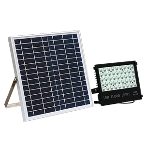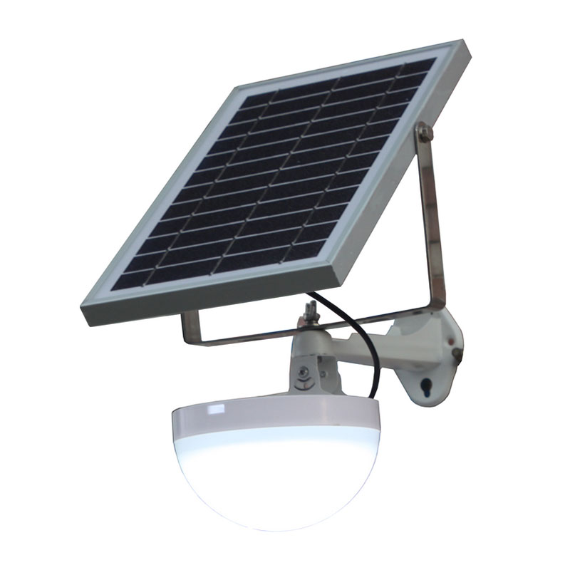
Outdoor solar lights that are ideal for environmental protection and power saving have become popular, and the prices of outdoor solar lights are also high to low. What determines the price? It is the cost of solar lamps. The cost of monocrystalline silicon also accounts for a part. Let us understand the monocrystalline silicon and its fabrication. For more questions, please click on the online consultation on the website, and you will have the first time to answer your questions.
Although silicon is stored in large quantities, they are not necessarily crystalline silicon, not necessarily monocrystalline silicon. So what exactly is monocrystalline silicon? Monocrystalline silicon is crystalline silicon and is a crystalline silicon with a substantially complete lattice structure. That is to say, the crystals are arranged in a regular pattern, which is a single crystal of silicon. The single crystal silicon rod produced by the Czochralski method is a relatively active non-metallic element and is an important component of the crystal material. At the forefront of the development of new materials, it is a good semiconductor, the most important and widely used elemental semiconductor material in the electronics industry and solar photovoltaic industry. The purity can reach 9.999%, even more than 99.999999%, for the manufacture of semiconductor devices, solar photovoltaic cells and the like.
Monocrystalline silicon is usually produced by first preparing high-purity polycrystalline silicon, and then using polycrystalline silicon as a raw material to prepare single crystal silicon. When solidified elemental silicon (polycrystalline silicon) is solidified, silicon atoms are arranged in a diamond lattice into a plurality of crystal nuclei. When the crystal nucleus has the same crystal orientation, the crystal grains are crystallized into single crystal silicon in parallel.
Monocrystalline silicon has the physical properties of a quasi-metal, has a weak conductivity, and its electrical conductivity increases with increasing temperature, and has a remarkable semiconductivity. In the ultra-pure single-product silicon, a levy of a group IIIA element is added. Boron can increase the degree of its conductivity, forming a P-type silicon semiconductor; if a small amount of VA elements such as phosphorus or arsenic are added, the degree of conductivity can be increased to form an N-type silicon semiconductor.
Monocrystalline silicon is usually produced by first preparing polycrystalline silicon or amorphous silicon, and then growing rod-shaped single crystal silicon from the melt by a Czochralski method or a suspension zone melting method. Monocrystalline silicon is mainly used to fabricate semiconductor components, such as semiconductor silicon devices, high-power rectifiers, high-power transistors, diodes, switching devices, etc., and can also be used to fabricate solar photovoltaic cells.
The production methods of single crystal silicon mainly include two types: the Czochralski method and the zone melting method, but the most common one is the Czochralski method. The zone melting method is divided into two types, one is the horizontal zone melting method; the other is the suspension zone melting method, and the common one is the suspension zone melting method.
The straight pull method is also divided into two types: one is a straight pull method; the other is a straight pull method, and now it is common to have a straight pull method.
(1) Straight pull method. In this method, the polycrystalline silicon for producing single crystal silicon is completely melted, and then the rotating seed crystal is brought into contact with the molten polycrystalline silicon liquid surface, and then the seed crystal is lifted upwardly at a uniform speed. During the upward pulling process, the polycrystalline silicon liquid is in the seed. Under the action of crystal, the crystals are rearranged, and the polycrystalline silicon which grows on the seed crystal and has a straight pull method is melted in the quartz crucible. The method has the advantages of simple process, easy equipment, safety and high production efficiency, especially It is capable of providing large diameter single crystals to meet certain special requirements.
However, there is a straight pull method, because the quartz crucible and the molten polysilicon act, the polysilicon will be contaminated, and the purity thereof will be correspondingly reduced. Despite this, the Czochralski method is still the most widely used method for producing monocrystalline silicon. The ballastless straight pull method is a combination of the Czochralski method and the suspension zone melting method, so that single crystal silicon having the advantages of the Czochralski method and the suspension zone melting method can be obtained (i.e., the single crystal having a small dislocation density, a low oxygen content, and a low compensation). ).
(2) Zone melting method. As the name suggests, it is local melting. The Czochralski method first melts all the polycrystalline silicon and then makes the seed crystals contact the molten polysilicon liquid surface. The zone melting method does not melt all the polysilicon, but makes the polycrystalline silicon for producing single crystal silicon contact with the seed crystal. Local melting begins with the polycrystalline silicon in contact with the seed crystal. The molten polycrystalline silicon liquid is subjected to seed crystals, the crystals are rearranged, and then slowly solidified into single crystal silicon. The heater moves slowly, so that the polysilicon melting zone moves slowly, melts the polysilicon little by little, and finally melts all the multi-product silicon, slowly turning the polysilicon into single crystal silicon.
The horizontal zone melting method is generally used for purifying tantalum and gallium arsenide, which is rare in the production of single crystal silicon. This is because the tension of single crystal silicon is large, and the current single crystal silicon wafer can be produced by the suspension zone melting method. According to the diameter of 6in, 8in, l2in (300mm) and 18in (450mm), the larger the diameter of the wafer, the more integrated circuits that can be engraved, the lower the cost of the film. But the larger the size of the chip, the higher the material and technology requirements. Single crystal silicon is divided into a Czochralski method (CZ), a zone melting method (FZ) and an epitaxial method according to different crystal growth methods. A single crystal silicon rod is grown by a straight pull method or a zone melting method, and a single crystal silicon film is grown by epitaxial method.
The single crystal silicon grown by the Czochralski method is mainly used for a semiconductor integrated circuit diode, an epitaxial wafer substrate, and a solar photovoltaic cell. At present, the crystal diameter can be controlled at ~8in. The district melting single crystal silicon is mainly used in the field of high voltage and high power controlled rectifier devices, and is widely used in high power transmission and transformation, electric locomotive, rectification, frequency conversion, electromechanical integration, energy saving lamps, TV sets and other products. At present, the crystal diameter can be controlled at 3~6in, and the epitaxial wafer is mainly used in the field of integrated circuits.
Due to cost and performance reasons, Czochralski (C2) single crystal silicon materials are the most widely used, and the materials used in the 1C industry are mainly CZ polishing sheets and epitaxial wafers. Memory circuits typically use Cz pads because of the lower cost. Logic circuits typically use higher cost epitaxial wafers because of their better applicability in IC manufacturing and the ability to eliminate the latch-up effect. Monocrystalline silicon, also known as silicon single crystal, is the most basic material in electronic information materials and belongs to the category of semiconductor materials.
Monocrystalline silicon has penetrated into various fields of national economy and national defense technology. Today, more than 95% of semiconductor devices and more than 99% of silicon for integrated circuits in the global telecom semiconductor market of more than 200 billion US dollars.
The strict control of the production process of monocrystalline silicon also determines the cost, which determines the price of outdoor solar lamps. Nuusolar has been processing wafers in a process consistent with national standards. Designed to create the best economical outdoor solar lights for our customers.

Copyright © 2017 Nuusolar